 (Hong Kong)

Product Summary
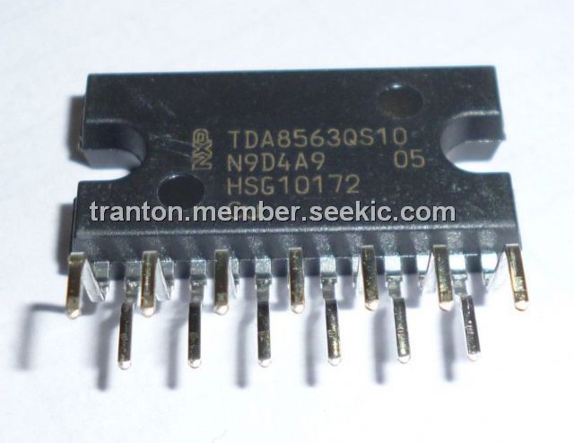
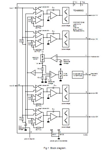
The TDA8563QS10 is an integrated class-B output amplifier in a 13-lead single-in-line (SIL) power package. It contains 2 × 40 W/2 Ω amplifiers in BTL configuration. The device is primarily developed for car radio applications.
Parametrics
TDA8563QS10 absolute maximum ratings: (1)VP supply voltage: 30 V; (2)Vpsc AC and DC short-circuit safe voltage: 18 V; (3)Vpr reverse polarity: 6V; (4)IOSM non-repetitive peak output current: 10 A; (5)IORM repetitive peak output current: 7.5 A; (6)Ptot total power dissipation: 60 W; (7)Tstg storage temperature: -55 to +150℃; (8)Tamb operating ambient temperature: -40 to +85℃; (9)Tvj virtual junction temperature: 150℃.
Features
TDA8563QS10 features: (1)Requires very few external components; (2)High output power; (3)4 Ω and 2 Ω load impedance; (4)Low output offset voltage; (5)Fixed gain; (6)Diagnostic facility (distortion, short-circuit and temperature detection); (7)Good ripple rejection; (8)Mode select switch (operating, mute and standby); (9)Load dump protection; (10)Short-circuit safe to ground, to VP and across the load; (11)Low power dissipation in any short-circuit condition; (12)Thermally protected; (13)Reverse polarity safe; (14)Electrostatic discharge protection; (15)No switch-on/switch-off plop; (16)Flexible leads; (17)Low thermal resistance.
Diagrams
 |
 TDA8000 |
Other |
|
Data Sheet |
Negotiable |
|
||||
|
TDA8000T |
Other |
|
Data Sheet |
Negotiable |
|
||||
|
TDA8001 |
Other |
|
Data Sheet |
Negotiable |
|
||||
|
TDA8002 |
Other |
|
Data Sheet |
Negotiable |
|
||||
|
TDA8002C |
Other |
|
Data Sheet |
Negotiable |
|
||||
|
TDA8002C/CD |
NXP Semiconductors |
I/O Controller Interface IC SMRT CRD INTERFCE IC |
Data Sheet |
Negotiable |
|
||||